DDR4/3, LPDDR
DDR5
Octa PSRAM
Winbond HyperRAM
UHS
- Compatible with following Xccela PSRAM devicesfrom APMemory ⋄ 8 bit data bus - DQ[7:0] support for APSxx08L-0B device, where xx stands for memory density ⋄ 16 bit data bus - DQ[15:0] support for APSxxyyN device, where yy stands for I/O config ⋄ Possible values: xx=64, 128, 256 and yy=08, 16
- Compatible with APS3208K device from APMemory
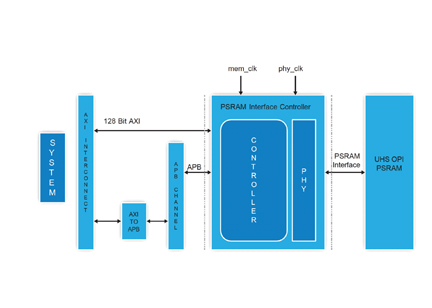
- Memory mapped access to the connected PSRAM Device
- Octal SPI Interface with DDR mode access support
- Wrap transfer support
- Continuous mode Burst transfer support for efficient memory access
- Hybrid wrap burst transfer support
- APB port for control registers accesses
- Read-Prefetch feature for efficient read data throughput in AHB-Lite flavour
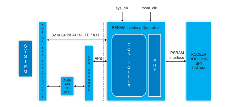
- AXI4 system interface for memory access with outstanding address support. Alternatively, AHB Lite system interface for memory access
- Half sleep and deep power down control through simple CSR access
- Behavioral reference PHY model for easier technology specific integration and implementation
Design Attributes
• Highly modular and programmable design • Fully synchronous design • Software control for key featuresProduct Package
• RTL Code • System Verilog/UVM based Testbench • Test cases • Protocol checkers and bus watchersDocumentation
• Design Guide • Verification Guide • Synthesis GuideLicensing Options
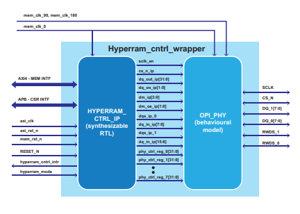
• Single Design or Multi-project license (HDL Source Code) - Compatible with W958D6NW, W958D6NKY, W956x8MBYA, W955D8MBYA HyperRAMTM devices from Winbond
- 16 bit data bus - DQ[15:0] support for W958D6NW, W958D6NKY devices
- 8 bit data bus - DQ[7:0] support for W956x8MBYA/ W955D8MBYA devices
- Read-Write data strobe RWDS [1:0]
- Memory Clock rate upto 250 MHz
- AXI memory mapped system interface for memory access.
- APB port for control registers accesses
- Supports Linear Burst, Hybrid burst and Wrap burst
- Low power features like deep power down, Hybrid sleep mode are handled by the controller through a CSR register.
Design Attributes
• Highly modular and programmable design • Fully synchronous design • Software control for key featuresProduct Package
• RTL Code • System Verilog/UVM based Testbench • Test cases • Behavioral PHY Model • Validated FPGA PHY reference designDocumentation
• Data-sheet • Verification PlanLicensing Options
• Single Design or Multi-project license (Encrypted RTL or HDL Source Code) -
Device Supported:
- Compatible with following UHS OPI PSRAM devices from APMemory - 8 bit data bus – DQ[7:0] support for AP325608AOKx device - 16 bit data bus – DQ[15:0] support for AP325616AOKx device Other Features:
- Memory mapped access to the connected PSRAM Device
- Octal SPI Interface with DDR mode access support
- Wrap transfer support
- Continuous mode Burst transfer support for efficient memory access
- Auto-initiate feature to reduce F/W overhead
- AXI4 system interface for memory access with outstanding address support.
- APB port for control registers accesses
- Features like Global Reset, Self Refresh and ZQ Calibration modes control through simple CSR access
- Reference PHY model for easier technology specific integration and implementation